PIC project using AD8950 DDS module for a direct conversion receiver
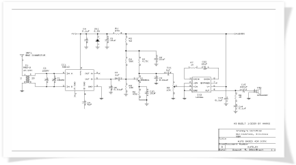
The design used for the VFO section of the DC receiver is published as opensource by Filipe LU5DJV and is available here. The PCB is a single sided board easily etched at home. The PIC source code ia available in HEX format on Filipe’s site.
The VFO is designed to be used as an RF generator from 0-
The receiver section uses a design from the QRP notebook by W1FB. I removed the original VFO circuit and injected the signal from the DDS on pin 6 of the SA612 via a 5pF capacitor.
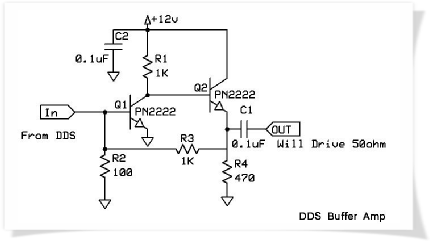
I found the signal from the DDS sufficient to drive the SA612 on 160/80/40m band, but needed a buffer for 30/20/10m. The buffer I used is pictured below.
73
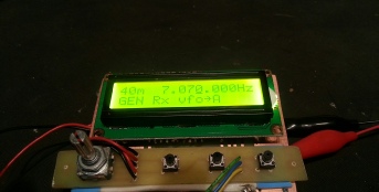
PIC 16F628A DDS VFO DC Receiver